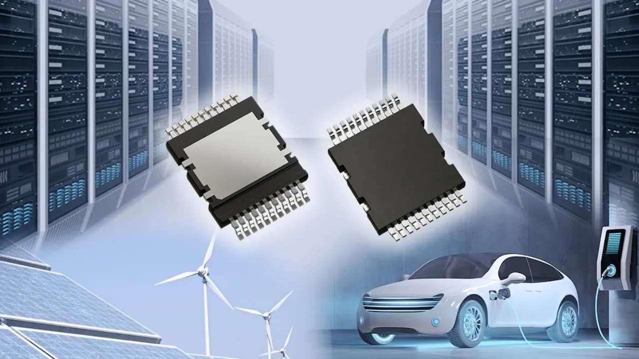
Toshiba Electronic Devices & Storage Corporation announced that it has started shipping test samples of its new 1200 V trench‑gate silicon‑carbide (SiC) MOSFET, part number TW007D120E. The device is targeted at power‑supply systems for next‑generation AI data centers and is also qualified for renewable‑energy equipment such as photovoltaic inverters and EV chargers. Toshiba plans mass production in fiscal 2026 and cites significant reductions in on‑resistance and switching loss as key efficiency drivers.
The Announcement
The TW007D120E MOSFET incorporates Toshiba’s proprietary trench‑gate structure, which the company says delivers industry‑leading low on‑resistance per unit area (RDS(on)A). Compared with Toshiba’s current 3rd‑generation SiC MOSFET (TW015Z120C), the new part reduces RDS(on)A by roughly 58 % and improves the figure of merit RDS(on) × Qgd by about 52 %. The device is packaged in a QDPAK that supports top‑side cooling, enabling higher power density and better thermal performance. Key electrical specifications include a typical RDS(on) of 7 mΩ at VGS = 15 V, a gate‑drain charge (Qgd) of 33 nC, and a drain current rating of 172 A at 25 °C. Toshiba will ship additional test units while preparing for full‑scale production in FY 2026 and intends to broaden the product line to automotive applications.
Why It Matters for the Energy Sector
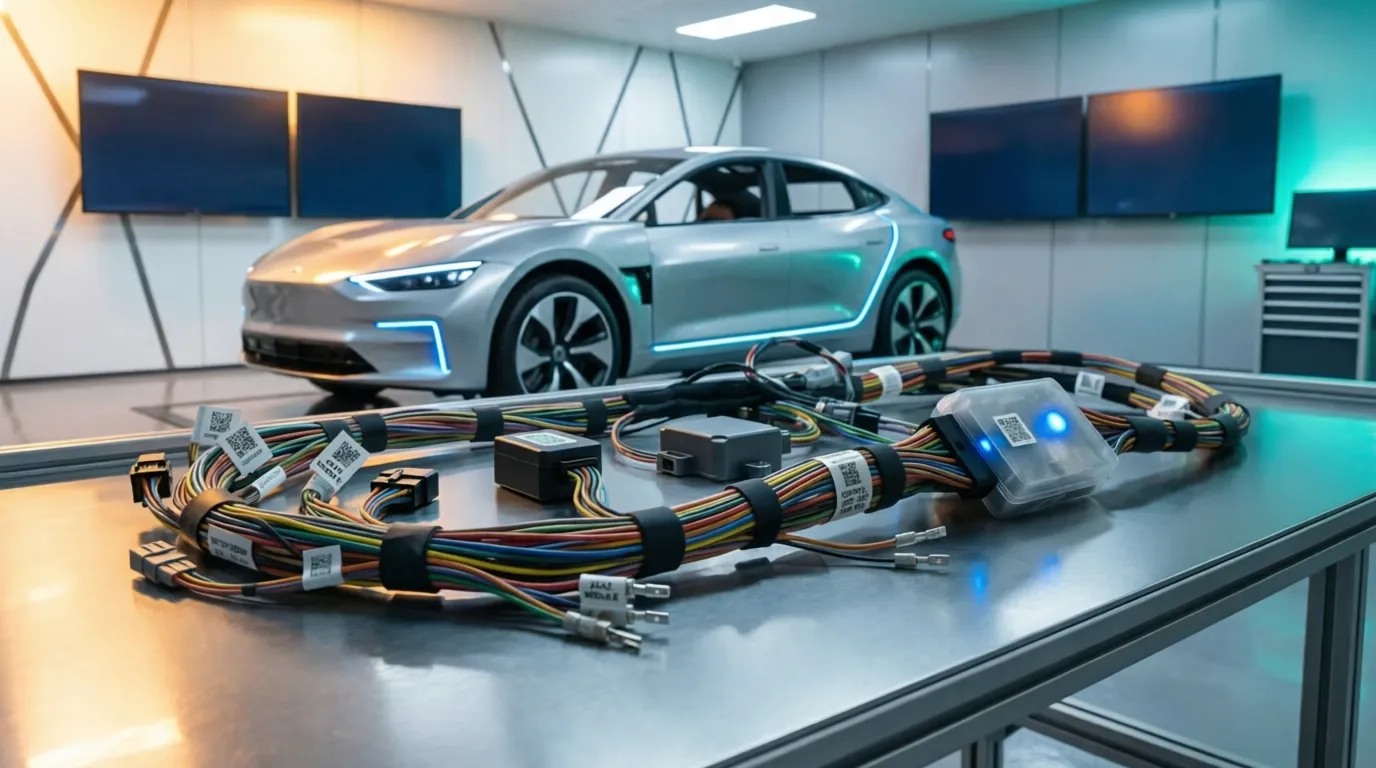
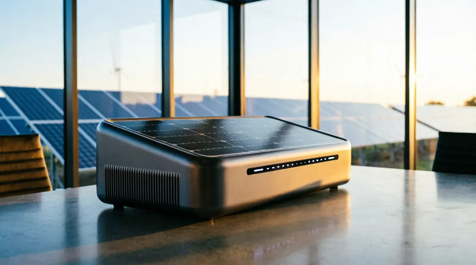
Data centers powering generative AI models are experiencing rapid growth in electricity demand. Higher‑voltage (800 V) DC architectures and high‑power AI servers require power converters that can operate with minimal losses. By lowering both conduction loss (through reduced RDS(on)A) and switching loss (via improved RDS(on) × Qgd), the TW007D120E can increase overall power‑supply efficiency and reduce heat generation. For operators, this translates into lower operating expenses, smaller cooling infrastructure, and a smaller carbon footprint—attributes that align with corporate decarbonization goals. The same efficiency gains are applicable to photovoltaic inverters, UPS systems, EV charging stations, and industrial motor drives, where SiC technology already offers advantages over silicon.
Grid, Supply, or Investment Context
The device’s development was supported by Japan’s New Energy and Industrial Technology Development Organization (NEDO) under project JPNP21029, indicating public‑sector interest in advancing SiC adoption. As utilities and industrial buyers seek to modernize grids with higher‑efficiency power electronics, the availability of a 1200 V SiC MOSFET with a high‑current rating (172 A) could accelerate retrofits of existing AC‑DC and DC‑DC converters. Supply‑chain considerations remain critical; while Toshiba is moving toward mass production in FY 2026, the timeline suggests a near‑term window for early adopters to secure test units and influence design specifications before broader market rollout.
What Comes Next
Toshiba will continue to qualify the TW007D120E for additional applications, notably automotive powertrains, and will expand its SiC MOSFET portfolio. Customers interested in the test samples should engage with Toshiba’s sales channels to assess integration requirements and thermal management solutions compatible with the QDPAK package. Monitoring the transition from test shipments to volume production will be essential for budgeting capital expenditures and planning system upgrades in data centers and renewable‑energy installations.
Key Takeaways
- Toshiba began shipping test samples of the 1200 V trench‑gate SiC MOSFET TW007D120E, aimed at AI data‑center power supplies and renewable‑energy equipment.
- The device reduces on‑resistance per unit area by ~58 % and improves the RDS(on) × Qgd figure of merit by ~52 % versus Toshiba’s prior 3rd‑generation SiC MOSFET.
- Mass production is targeted for fiscal 2026, with plans to extend the technology to automotive applications.
EnergyInsyte's Take
The launch of Toshiba’s TW007D120E signals a tangible step toward higher‑efficiency power conversion in AI‑driven data centers, a segment where electricity costs are a major operating expense. Decision‑makers should evaluate the thermal and electrical benefits of the trench‑gate SiC MOSFET against existing silicon solutions, especially when designing next‑generation 800 V DC architectures. Early engagement with Toshiba can secure test hardware and influence product qualification timelines, reducing risk for large‑scale deployments. However, the commercial impact will depend on how quickly the company scales production and on the broader SiC supply chain’s ability to meet demand across data‑center, renewable, and automotive markets. Continuous monitoring of volume‑production milestones and pricing structures will be crucial for capital‑allocation decisions.
Source: Businesswire